Introduction
Microfluidics is the manipulation of fluids where at least one dimension is less than a millimeter. In simpler terms, microfluidics can be thought of as plumbing on a micro-scale. Drug discovery and diagnostics are two fields that have benefited greatly from microfluidics.
In biological settings, microfluidics allows direct control of the environment surrounding biological cells, including delivery of different concentrations of nutrients, precisely controlled velocity profile, and shear forces. These advantages have made microfluidics a core technology in new platforms for drug discovery. By culturing cells in 3D environments more closely imitating their native environment, the response of cells to drugs are more relevant than when cultured in traditional 2D petri dishes. Novel therapies involving stem cells have also benefited greatly from microfluidics – stem cell differentiation to heart or bone cells relies on precisely controlled pulsatile fluid flow and shear forces.
Microfluidics is also used to automate diagnostic assays to improve efficiency and speed, as well as to reduce cost. Microfluidics enables one to perform analysis using smaller samples, and therefore, the same assays can be performed using less reagents, leading to further cost saving. There are a myriad of portable microfluidic technologies developed for point of care diagnostics, some are as simple as the ubiquitous glucose meters, and others are more advanced, such as the ID NOW(TM) COVID-19 rapid test by Abbott.
With the growing popularity of microfluidics, there is a need to manipulate cells, which is challenging with current microfluidic technologies. The purpose of this whitepaper is to shed light on how the integration of patterned illumination can add value to microfluidics for applications such as enabling single cell manipulation and cell sorting.
Microfluidics and the Need for Cell Manipulation
Microfluidic devices based on micro-channels, as shown in figure 1 (a), are the most popular type of microfluidics because prototyping is fast and cheap using soft lithography and it provides a great degree of control. A popular method to control the flow is using a syringe pump to provide pressure-driven flow. A syringe filled with fluid is connected to the inlet and then the syringe is pushed. At the micro-scale, laminar flow, as opposed to turbulent flow, dominates.
A common experiment that demonstrates the advantage of laminar flow is the ability to deliver different reagents to different parts of a microfluidic channel. For applications that require precise control, a flow meter or pressure sensor can be used to provide feedback and modify the pressure or flow rate. Additionally, it is possible to integrate valves and pumps in the microfluidic chip itself – this is particularly important when many different fluids are being controlled simultaneously [1].
The main challenge with these microfluidic devices is the limited ability to manipulate individual cells. Cells suspended in fluid move with the moving fluid in bulk. The force causing cell motion is only the viscous drag force acting on all cells due to the moving fluid, offering no means to manipulate individual cells of interest.
In the example of drug discovery, being able to isolate single cells or small groups of cells that respond in a particular way to a drug will enable in depth understanding by downstream analysis such as protein expression or RNA sequencing of a single cell or small number of cells of interest.
In the example of diagnostics, cell sorting can be used to isolate bacteria or circulating tumor cells. While there are other technologies that have accomplished these single cell manipulations, lack of integration with microfluidics has limited the usefulness of these technologies.
The development of a technique called optoelectronic tweezers, based on optical patterned illumination, can help overcome the challenges associated with cell manipulation in microfluidics. As will be described in the next section, the architecture of optoelectronic tweezer devices lends themselves to easy integration with microfluidics.
Optoelectronic Tweezers – Cell Manipulation Using Patterned Illumination
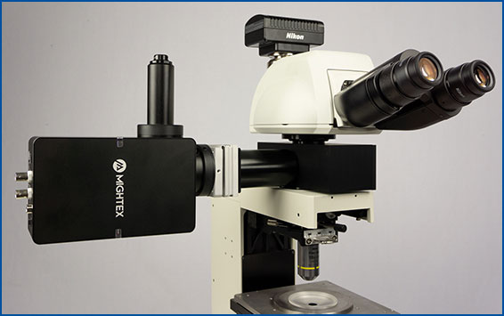
By using a photoconductive material, patterned illumination can be used to create virtual electrodes post-fabrication. Patterned illumination refers to a software-programmable pattern of light, generated using an optical patterned illuminator, such as Mightex’s Polygon DMD illuminator, based on a digital micromirror array device (DMD). A light pattern can be simple stationary shapes, such as lines, circles, donut-shapes, or can be dynamic like moving light bars. This mechanism is the core of optoelectronic tweezers (also known as optically-induced Dielectrophoresis) [2].
A typical optoelectronic tweezer device is shown in figure 1 (b). It is composed of a bottom and a top plate as shown on figure 1 (c). The bottom plate has a photoconductive layer on top of an unpatterned electrode – a popular photoconductive material is hydrogenated amorphous silicon (a-Si:H). The photoconductive layer has a high resistance in dark conditions and acts as an insulator. The top plate has a transparent conductor, such as indium tin oxide (ITO), forming a second electrode. An AC signal is applied across the device using the bottom and top electrodes, forming a uniform electric field in dark conditions.
A light pattern on the photoconductive layer causes a local reduction in the resistance due to generated electron-hole pairs. The illuminated region becomes a virtual electrode. The electric field is no longer uniform across the bottom and top plates. This non-uniform electric field induces a dielectrophoretic force on cells/particles that can be described by equation (1).

Where r is the radius of the particle being manipulated, ∇E^2 is the gradient of the electric field squared, K(ω) is the frequency-dependent Claussius Mossotti factor. K(ω) is a measure of the polarizability of the particle, and it depends on the complex permittivity of the particle ε_p^* and the medium surrounding it ε_m^*.
This effect is reversible; when the illumination is turned off, the electron-hole pairs recombine, and the resistance returns to its original state, i.e. the photoconductor becomes an insulator again.
The size, shape and location of these virtual electrodes can be defined on the fly. Modern DMD devices, such as the Mightex’s Polygon DMD Illuminator, have over a million pixels, and it is possible to illuminate multiple unique shapes simultaneously. Each shape defines a virtual electrode, controlling cells with high versatility, depending on the application. The electrode shape can be defined to trap a single cell or a population of cells, and cells can be trapped and moved.

Figure 1. (a) Channel microfluidic device (cross-section), (b) Cross section of Optoelectronic tweezer device, (c) simple assembly of optoelectronic tweezer device by sandwiching spacer (typically double-sided tape) between bottom and top plates.
Integrating Optoelectronic Tweezers with Microfluidics: A Marriage of Practicality
Early experiments with optoelectronic tweezers had a device that looked a lot like that in figure 1 (b), with no real integration with microfluidics. Such setup is sufficient for proof-of concept experiments. However, for more useful real-life applications, control of fluid flow is essential.
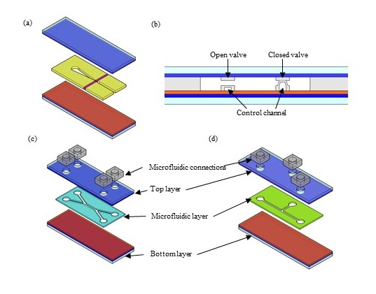
The first reports showing integration of microfluidic channels in optoelectronic tweezer devices used SU-8 [3] and poly-dimethyl-siloxane (PDMS) [4], [5], shown in figure 2 (a-c). One method to use PDMS is to transform the surface of PDMS to be conductive by using a gold mesh [6] or single walled carbon nanotubes (SWNT) [4], [6], figure 2 (b). The conductivity is worse than that of ITO however, and other methods that do not deviate that much from the architecture in Fig 1 (b) have become more popular. Channels can be defined in thin PDMS sheets that are sandwiched between the two plates of the optoelectronic tweezer device, such as in Figure 2 (c) [5]. Either way, PDMS integration allows incorporating valves and pumps inside the device. Figure 2 (c) (iii). shows that cells of interest can be “parked” into a side channel and then a PDMS valve can be opened to allow mixing with reagents.
Double-sided tape seems to be gaining popularity, with primarily three methods of patterning: (1) laser cutting (Figure 2 (d)) [7], (2) metal punching (Figure 2 (e)), i.e. pressing a metal mold to the tape (just like a “cookie-cutter”) [8], (3) xurography, i.e. cutting with a blade. The next section will describe in more depth some example applications that were enabled by the integration of optoelectronic tweezers and microfluidics.

Figure 2. Methods for integrating microfluidics with optoelectronic tweezers. In this schematic, glass is shown in light blue, ITO in dark blue and amorphous silicon in red. (a) Microfluidic channel defined by photolithography of SU-8 (shown in golden) followed by bonding using epoxy. Optical fibers (shown in purple) were integrated for optical interrogation of particles [3]. (b) Thin layers of PDMS (shown in grey) used to define microfluidic channel and valves. Valve is open when air pressure in control channel is low and is closed when air pressure in control channel is high [5]. (c) Microfluidic channel defined by laser cutting of double sided tape (shown in cyan), sandwiched between bottom and top layers [7], (d) microfluidic channel defined by pressing metal mold to double sided tape (“cookie cutter” approach) – microfluidic layer in green – and sandwiching between bottom layer and top layer; The microfluidic connections layer consists of inlets and outlets [8].
Applications of Optoelectronic Tweezers
Cell Sorting
While there are a variety of other techniques capable of size-based cell sorting, each application requires a new microfluidic chip. Using optoelectronic tweezers for size-based cell sorting means that mass scale production can be employed, and then each chip can have the sorting capabilities tuned for its application.
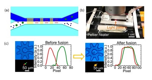
In cases where the sample volume is small or for initial proof-of-concept experiments, cell sorting can be performed on an open platform without a microfluidic channel, such as [9] as shown in figure 3 (a). Solutions integrating optoelectronic tweezers with microfluidic channels are more useful. Figure 3 (b) shows a top inlet channel delivering medium only while the bottom inlet channel delivers the sample to be sorted. In microfluidics, there is no turbulence – laminar flow dominates – and thus mixing between these two streams is only due to diffusion. Therefore, in the absence of perturbations, the sample remains in the stream that is graphically represented in white. There is no physical barrier between the two streams. Dynamic light patterns are used to push the larger cells to the stream for large cell collection (the blue area in figure 3 (b-c)). This has been used to isolate circulating tumor cells [7], separate dead from live cells [10] and separate viable immotile sperm cells from dead immotile sperm cells [11].

Figure 3. (a) Integrating OET technology with microfluidics using laser-cut double-sided tape. Sample containing tumor cells (depicted in green) introduced from lower channel – after optoelectronic tweezer manipulation, tumor cells directed to upper channel [7]. (b) Microfluidic channel defined by xurography of double-sided tape integrated in optoelectronic device. After manipulating single cells, cells can be cultured, extracted for downstream analysis such as RNA sequencing and combined for electrofusion experiments (c).
Cell Trapping
Individual cells of interest can be identified, trapped and moved by a light pattern, for example a donut shaped light pattern [12], [13]. This allows picking specific cells out of a population of heterogeneous cells. When compared to cell sorting explained earlier, cell sorting relies on different properties of cells, such as size or dielectric properties – the dielectric force is stronger on larger cells than small cells. However, for many applications, this is not the case, and cells are not distinguishable by size or dielectric properties, but instead can be distinguished by other means such as a fluorescence signal or cell morphology. Optoelectronic tweezers can be used as a single cell manipulation tool without the complexities and limitations associated with microactuators or optical tweezers.
The introduction of the optoelectronic microrobot can vastly improve the functionality of optoelectronic tweezers with single cell manipulation. Small cells are harder to move than large cells, and manipulation speed is only a few microns per second when working with small cells. In a real application, many such cells must be transported several mm or even cm away from a heterogeneous population. Additionally, viability of cells can be compromised by optoelectronic tweezer operation. Instead, optoelectronic microrobots can be used [14]. In this case, cells are loaded inside microrobots, the patterned illumination creates virtual electrodes that move microrobots. This approach allows moving small cells easily. Additionally, the sharp non-uniform electric field does not interface cells directly but instead interfaces the microrobots, and the viability is not compromised. In [14], after trapping and moving a single cell away from a population, it was possible to perform a variety of applications, such as analysing RNA expression from a single cell, single cell clonal expansion, and combining two different cells and performing electrofusion experiments using the device shown in figure 3 (d). Figure 3 (e) shows an electrofusion experiment that was only possible due to this marriage of microfluidics and optoelectronic tweezers. Microfluidic channels were defined in double sided tape using xurography. First, cells of interest were brought to one another using optoelectronic tweezers, then electrofusion media was introduced using flow control, enabled by microfluidic integration. Finally, electric pulses were activated to complete the electrofusion process.
Challenges
Fabrication challenges for optoelectronic tweezer integration with microfluidics. When integrating a microfluidic channel inside a two-plate device, there is still not an established robust method that ensures leak-free operation. As illustrated in figure 3, double sided tape can be used, but there are inherent resolution limitations because the patterning is based on xurography or laser cutting instead of photolithography. Photolithographically-defined SU8 can be used is in Fig. 3 (d), but the SU8 was developed while between the bottom and top plates – this requires the microchannels to be quite large to allow the developer to reach the uncured areas without overdeveloping.
Optoelectronic tweezer in high conductivity media. Cell culture media typically have conductivity higher than 1 S/m, and this requires that the conductivity of the illuminated region be higher than that. The easier and more popular method of using an unpatterned photoconductive layer requires a very strong light intensity of several W/cm2 to achieve such high conductivity. In addition to the technical difficulties this method involves, such high optical power can potentially damage cells, and an alternative is to use an array of phototransistors [15].
Biofouling. Another challenge is that a large component of the DEP force in the typical optoelectronic device in figure 2 is in the vertical (z) direction. At high applied voltages, this can cause cells to stick to the bottom of the device. Some workarounds include anti-fouling layers, but these can reduce the DEP force that the cells see [16]. Another solution is lateral optoelectronics devices [17], in which interdigitated electrodes are used instead of unpatterned electrodes. This leads to lateral electric field rather than vertical. In addition to providing a stronger force in the x-y plane, the absence of a top plate means it is easier to incorporate a microfluidic channel. This approach suffers from reduced versatility however, as cells cannot easily move anywhere on the chip, but it may be useful for certain applications.
Conclusion
Microfluidic technologies enable controlling the environment surrounding cells and enable automation of diagnostic assays. Manipulating single cells in microfluidic devices is challenging; however, using patterned illumination can simplify single cell studies with microfluidics. Optoelectronic tweezer technology uses patterned illumination to define virtual electrodes and induce Dielectrophoresis forces. A DMD-based patterned illuminator gives a strong dark-light contrast and enables strong gradient of electric field and strong DEP forces. In addition to stationary light patterns, dynamic software-programmable light patterns can be used for high throughput cell sorting and manipulation of several single cells simultaneously.
Authors: Mohammed Elsayed (University of Toronto) & Jacob Cloke (Mightex)
Interested in Microfluidics and Patterned Illumination?
Click here to learn more about Mightex’s Polygon DMD illuminator.

References
[1] T. Thorsen, S. J. Maerkl, and S. R. Quake, “Microfluidic Large-Scale Integration,” Science (80-. )., vol. 298, no. 5593, pp. 580–584, Oct. 2002.
[2] E. P. Y. Chiou and M. C. Wu, “Optoelectronic Tweezers,” Micro/Nano Technol. Syst. Biomed. Appl. Microfluid. Opt. Surf. Chem., vol. 9780199219, no. June, pp. 8–10, 2010.
[3] Y. H. Lin and G. Bin Lee, “Optically induced flow cytometry for continuous microparticle counting and sorting,” Biosens. Bioelectron., vol. 24, no. 4, pp. 572–578, Dec. 2008.
[4] K. W. Huang, Y. C. Wu, J. A. Lee, and P. Y. Chiou, “Microfluidic integrated optoelectronic tweezers for single-cell preparation and analysis,” Lab Chip, vol. 13, no. 18, pp. 3721–3727, Aug. 2013.
[5] K. W. Huang, Y. C. Kung, Y. C. Wu, Y. J. Fan, and P. Y. Chiou, “Optoelectronic tweezers integrated with 3D microfluidic networks,” in International Conference on Optical MEMS and Nanophotonics, 2013, pp. 79–80.
[6] K. W. Huang, S. Sattar, J. F. Zhong, C. H. Chou, H. K. Tsai, and P. Y. Chiou, “Electrodes for microfluidic integrated optoelectronic tweezers,” Adv. Optoelectron., vol. 2011, 2011.
[7] S. Bin Huang et al., “High-purity and label-free isolation of circulating tumor cells (CTCs) in a microfluidic platform by using optically-induced-dielectrophoretic (ODEP) force,” Lab Chip, vol. 13, no. 7, pp. 1371–1383, Apr. 2013.
[8] T. K. Chiu et al., “Optically-induced-dielectrophoresis (ODEP)-based cell manipulation in a microfluidic system for high-purity isolation of integral circulating tumor cell (CTC) clusters based on their size characteristics,” Sensors Actuators, B Chem., vol. 258, pp. 1161–1173, Apr. 2018.
[9] W. Liang et al., “Rapid and Label-Free Separation of Burkitt’s Lymphoma Cells from Red Blood Cells by Optically-Induced Electrokinetics,” PLoS One, vol. 9, no. 3, p. e90827, Mar. 2014.
[10] H. Song-Bin, L. Shing-Lun, L. Jian-Ting, and W. Min-Hsien, “Label-free Live and Dead Cell Separation Method Using a High-Efficiency Optically-Induced Dielectrophoretic (ODEP) Force-based Microfluidic Platform,” Int. J. Autom. Smart Technol., vol. 4, no. 2, pp. 83–91, 2014.
[11] A. T. Ohta et al., “Motile and non-motile sperm diagnostic manipulation using optoelectronic tweezers,” Lab Chip, vol. 10, no. 23, pp. 3213–3217, 2010.
[12] S. Zhang et al., “Patterned Optoelectronic Tweezers: A New Scheme for Selecting, Moving, and Storing Dielectric Particles and Cells,” Small, vol. 1803342, p. 1803342, 2018.
[13] S. Zhang et al., “Size-scaling effects for microparticles and cells manipulated by optoelectronic tweezers,” Opt. Lett., vol. 44, no. 17, pp. 146–9592, 2019.
[14] S. Zhang et al., “The optoelectronic microrobot: A versatile toolbox for micromanipulation,” Proc. Natl. Acad. Sci., p. 201903406, Jul. 2019.
[15] A. Jamshidi et al., “An integrated single cell optofluidic platform based on phototransistor optoelectronic tweezers,” in Optics InfoBase Conference Papers, 2010.
[16] A. N. K. Lau et al., “Antifouling coatings for optoelectronic tweezers,” Lab Chip, vol. 9, no. 20, pp. 2952–2957, Oct. 2009.
[17] C. F. Song, K. Chen, and Z. H. Ni, “Analysis of Influence of Optical Electrode Geometry Effects on Manipulation Using Lateral-Field Optoelectronic Tweezers,” Adv. Mater. Res., vol. 194–196, pp. 2444–2447, Feb. 2011.


